


What Is Depletion Region?
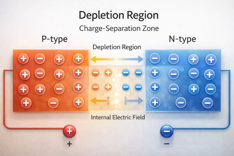
A depletion region is a thin zone that forms at the boundary between p-type and n-type semiconductor materials in a P-N junction. In this region, mobile charge carriers such as free electrons and holes have diffused away and recombined, leaving behind fixed ionized atoms in the crystal lattice. Because free carriers are largely absent, the region becomes electrically depleted and develops an internal electric field.
This internal electric field creates a directional barrier that influences how charges move through the junction. When electrons and holes approach the boundary, the field pushes them in opposite directions, establishing an equilibrium that prevents further large-scale diffusion. In semiconductor systems such as photovoltaic charge-separation structures, the depletion region plays a central role by separating electron-hole pairs generated by incoming photons and guiding them toward opposite electrical contacts.
The width and strength of the depletion region depend on factors such as doping concentration, temperature, and applied voltage. Engineers control these parameters to tune how semiconductor devices behave in applications ranging from diodes and transistors to solar cells and photodetectors.
Example:
In a silicon diode, the depletion region acts as an internal electric barrier that allows current to pass more easily in one direction than the other.
Related Concepts:
- P-N Junction
- Built-In Electric Field
- Electron-Hole Pair
NoSuchDevice is a free archive of machines that do not exist yet but already have a shadow in physics. I research and write every entry alone, with no ads. Take a look around the archive, or help keep it free.