


What Is P-N Junction?
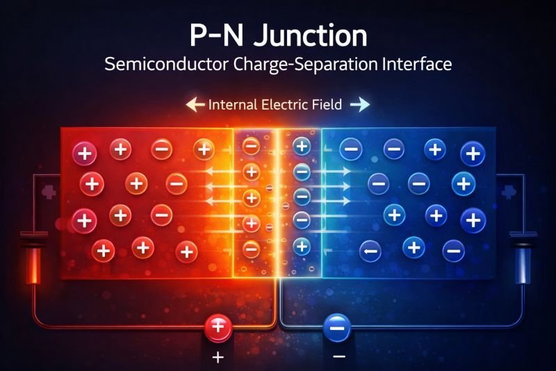
A P-N junction is the boundary formed where two regions of a semiconductor with different electrical properties meet. One side is doped to contain an excess of electrons (n-type), while the other contains an excess of holes, which act as positive charge carriers (p-type). When these regions come into contact, electrons and holes diffuse across the boundary and create a thin zone depleted of free carriers. This region forms an internal electric field that strongly influences how charges move through the material.
The electric field inside the depletion region acts as a directional barrier that allows charge carriers to move more easily in one direction than the other. This asymmetric behavior is the physical basis of diodes, transistors, and many optoelectronic devices. In semiconductor energy systems such as photovoltaic charge-separation architectures, the P-N junction separates electron-hole pairs created by incoming photons, guiding electrons and holes toward different electrical contacts.
The junction’s behavior depends on factors such as doping concentration, temperature, and applied voltage. By controlling these parameters, engineers can design semiconductor devices that rectify current, detect light, regulate voltage, or convert radiant energy into electrical power.
Example:
A silicon diode conducts electrical current primarily in one direction because its internal structure is built around a P-N junction.
Related Concepts:
- Depletion Region
- Electron-Hole Pair
- Semiconductor Doping
NoSuchDevice is a free archive of machines that do not exist yet but already have a shadow in physics. I research and write every entry alone, with no ads. Take a look around the archive, or help keep it free.