
At noon in June, the south-facing wall of a four-story apartment block absorbs over 100 kilowatts of solar radiation. By evening, every watt has turned into heat. The paint on that wall is doing exactly what paint has done for centuries – reflecting a color, protecting the substrate, and ignoring the energy that hits it. Nobody designing that coating ever thought about catching photons, because until recently, no pigment particle could produce a voltage.
Semiconductor nanoparticles changed that. Quantum dots smaller than 10 nanometers can absorb photons and release electrons, and their absorption frequency is tunable by adjusting particle size. Mix them into a binder, apply the result to a wall, and the surface begins generating electricity. The concept is not a solar panel bolted to a building.
It is the building itself becoming the panel.
The short version: Photovoltaic nanoparticles suspended in paint can convert sunlight to electricity on any coated surface. A four-story apartment block with all exterior walls and roof painted at 10% conversion efficiency could generate over 50,000 kWh per year – roughly 74% of its total residential consumption. No mounting hardware, no structural modification, no dedicated roof space.
Key Takeaways
- A vertical south wall receives less sunlight per square meter than a roof, but most buildings have far more wall area than roof area – and the geometry nearly cancels out
- Quantum dots can be tuned to specific light frequencies by changing their diameter by a few nanometers, which means layered paint coats could work like multi-junction solar cells applied with a roller
- Collecting current from a painted wall requires a conductive underlayer thinner than a sheet of paper, connected by electrode strips to the building’s inverter
- A single apartment block painted on all sides could offset most of its electricity consumption before any behavioral change or storage optimization
- At city scale, millions of painted buildings stop being consumers and become a distributed power surface – a shift that changes what an electrical grid is for
Table of Contents
How Sunlight Hits a Building and What Gets Wasted
Solar panels go on roofs because roofs face the sky. That logic is so obvious it has prevented almost everyone from asking a different question: what about the rest of the building?
The Vertical Wall Problem
A horizontal surface perpendicular to incoming sunlight captures the maximum flux. A vertical wall cannot do that except briefly at sunrise and sunset, when the sun is near the horizon and the intensity is low. At solar noon, when irradiance peaks, the south wall of a mid-latitude building catches only 50 to 70 percent of what a horizontal rooftop receives. Engineers designing conventional solar panels would call that unacceptable. For a coating that costs a fraction of a panel and covers ten times the area, the arithmetic looks different.
Watts Per Square Meter Across the Building Envelope
Not every face of a building contributes equally. A four-story block with a flat roof of 200 square meters and four walls averaging 120 paintable square meters each (after subtracting windows) exposes roughly 680 square meters of surface to the sky. The useful output depends on orientation and local irradiance.
| Surface | Avg daily irradiance (kWh/m²) | Paintable area | Daily yield at 10% efficiency |
|---|---|---|---|
| South wall | 2.5 | 120 m² | 30.0 kWh |
| East wall | 1.5 | 100 m² | 15.0 kWh |
| West wall | 1.5 | 100 m² | 15.0 kWh |
| North wall | 0.6 | 120 m² | 7.2 kWh |
| Flat roof | 3.5 | 200 m² | 70.0 kWh |
The total is 137 kWh per day. The north wall contributes the least in absolute terms, but its 7.2 kWh still exceeds zero, which is what every unpainted north wall produces now. Diffuse skylight is weak, but it is not nothing, and a surface that harvests it for free has no minimum threshold to justify its existence.
Nanoparticles That Catch Photons at Tunable Frequencies
The photovoltaic effect in bulk silicon requires a rigid crystal lattice, a fixed bandgap of 1.12 electron-volts, and a wafer thick enough to absorb incoming light. Semiconductor nanoparticles operate on the same physical principle but add a variable that bulk materials cannot offer: quantum confinement.
Quantum Dots and the Size-Frequency Relationship
A quantum dot is a semiconductor crystal small enough that its electronic properties depend on its physical dimensions. A cadmium selenide particle 2 nanometers across absorbs blue light. Grow it to 6 nanometers and it absorbs red. The bandgap shifts because the electron’s confinement energy changes with the box it occupies – smaller box, higher energy gap, shorter wavelength absorbed. The same material, synthesized at different sizes, covers different parts of the solar spectrum.
Suspend these particles in a polymer binder and the result is a liquid that can be applied like paint. Once dried, the film contains billions of nanoscale photovoltaic junctions per square centimeter. Each dot absorbs a photon and generates an electron-hole pair. The challenge is getting those carriers out of the film and into a circuit before they recombine, but the principle is identical to what happens inside a rooftop panel. Only the geometry has changed.
Layered Paint as a Multi-Junction Solar Cell

A single layer of quantum dots tuned to one frequency captures that slice of the spectrum and lets the rest pass through or reflect. Stack three layers – one optimized for blue-violet, one for green-yellow, one for red-infrared – and the combination absorbs across most of the solar spectrum. Each layer contributes voltage from its own spectral band.
In conventional photovoltaics, multi-junction cells are among the most expensive devices ever manufactured. They require epitaxial growth of lattice-matched semiconductor layers in vacuum chambers. The paint version sidesteps that process entirely. Each layer is a separate coat applied at atmospheric pressure. The lattice matching problem disappears because quantum dots are not lattice-bonded to each other. Precision that costs thousands of dollars per square centimeter in a III-V multi-junction cell reduces to particle size control during chemical synthesis.
Where the Shockley-Queisser Ceiling Bends
A single-junction solar cell has a theoretical efficiency limit of 33.7 percent. That number comes from the Shockley-Queisser calculation, which accounts for thermalization losses (photons with too much energy waste the excess as heat) and transmission losses (photons with too little energy pass through unabsorbed). Every photon that does not match the bandgap is either partially or completely wasted.
Stacking Spectral Bands in a Paint Film
Multi-junction architectures break past that ceiling by splitting the job among layers with different bandgaps. A two-layer stack raises the theoretical maximum to roughly 42 percent. A three-layer stack reaches about 49 percent.
The formula that governs the electrical output of any photovoltaic surface is straightforward:
P = G x A x η
Where P is electrical power in watts, G is solar irradiance on the surface in W/m², A is the active painted area in square meters, and η is conversion efficiency.
For a south-facing wall at noon receiving 600 W/m², with 120 square meters of paint at a three-layer efficiency of 15 percent: P = 600 x 120 x 0.15 = 10,800 watts. That is 10.8 kilowatts from one wall at midday – enough to run thirty household air conditioning units simultaneously. Raise the efficiency to the theoretical three-layer ceiling, and the same wall crosses 35 kilowatts. The surface area has not changed. The building has not been modified. Someone applied three coats of paint.
Everything here is free. Readers are the reason it stays that way.
I make all of it alone, with no ads. If it is worth a coffee a month to you, that keeps the next one coming.
Keep it alive →Collecting Current From a Painted Surface
Generating electron-hole pairs inside a film of nanoparticles is only useful if the current can reach a wire. A photovoltaic paint system needs two electrodes sandwiching the active layers, and at least one of them must be transparent enough to let sunlight through.
Conductive Underlayers and Mesh Electrodes
The bottom electrode sits between the building wall and the first paint layer. Transparent conductive oxides like indium tin oxide have been used in thin-film photovoltaics for decades, but spray-coatable alternatives – carbon nanotube films, silver nanowire meshes, conductive polymers – suit a paint-based system better. The underlayer needs a sheet resistance below 10 ohms per square and optical transparency above 80 percent. Carbon nanotube coatings already meet both numbers in laboratory conditions.
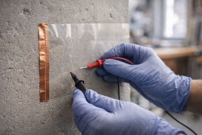
On top of the outermost paint layer, a second conductive film collects the current. Thin silver nanowire mesh, applied as a final clear coat, can serve this role without visibly altering the surface. The sandwich – bottom electrode, three paint layers, top electrode – is thinner than a credit card and bonds directly to the substrate.
From Wall to Inverter – Wiring a Building Envelope
Copper bus bars run along the edges of each painted section, gathering current from the electrode layers and feeding it into conventional wiring concealed in the wall structure. From there, the path is identical to a standard rooftop solar installation: DC current flows to an inverter, the inverter outputs AC, and the building either consumes the power or pushes it to the grid.
The inverter architecture changes slightly because current arrives from multiple orientations – south wall, east wall, roof – at different voltages and generation profiles throughout the day. Micro-inverters assigned to each facade section handle this more cleanly than a single central unit, and they allow one wall to operate independently if another is shaded or damaged.
Rolling It On – How Application Shapes the Circuit
A quantum dot film that varies in thickness by even a few micrometers produces uneven current density. Thick spots absorb more light but increase internal resistance. Thin spots let photons through uncaptured. The application method is not a construction detail – it is an electrical engineering constraint.
Homogeneity and Why Gaps Kill Current

Spray coating under controlled conditions produces the most uniform films. Industrial electrostatic sprayers, already used for automotive paint, can hold thickness variation within plus or minus 2 micrometers across a flat panel. Scaling that precision to a four-story wall with window frames, drainage pipes, and surface irregularities is a different problem. Roller application introduces streak patterns. Brush application is out of the question for any area meant to generate meaningful power.
The likely path for early deployment is factory-coated panels – lightweight substrates pre-painted under controlled conditions, then attached to building facades like cladding. Later generations may use robotic spray systems that map the wall surface, adjust nozzle distance in real time, and verify film thickness with inline optical sensors. Applying a three-layer multi-junction coating by hand, uniformly, across an entire building is probably the last method that becomes practical. The irony is worth noting: the simplest-sounding application (paint a wall) demands the most sophisticated process control.
One Apartment Block, One Calculation

A residential block with 16 apartments in a mid-latitude European city. Four stories, flat roof, windows covering roughly a third of each wall face. Total paintable exterior surface: 680 square meters. Average electricity consumption per apartment: 350 kWh per month. Building total: 5,600 kWh per month, or 67,200 kWh per year.
At 10 percent paint conversion efficiency, the painted building generates approximately 137 kWh per day across all surfaces. That is 50,000 kWh per year – roughly 74 percent of total consumption.
At 15 percent efficiency, the yield rises to 75,000 kWh per year. The building now produces 112 percent of what it consumes. It has flipped from grid consumer to net generator, and nobody installed a single solar panel. The surface that was already there, already maintained, already repainted every decade, is doing the work.
Seventy-four percent coverage at a conversion efficiency that quantum dot cells have already demonstrated in laboratory settings. One hundred and twelve percent at an efficiency that multi-junction paint architectures make physically plausible within two decades. Those numbers reframe the conversation. The question stops being “can solar paint contribute?” and becomes “how much conventional generation does it displace?”
From Solar Paint to Active Infrastructure Surfaces
Photovoltaic paint on a single building is a seed technology. The device it becomes at scale is something larger: the active building envelope, a system where every constructed surface participates in energy generation as a default function of its material composition.
What Happens When a Million Buildings Generate Power
A mid-sized European city has on the order of 100,000 to 300,000 buildings. If the average building contributes even 30,000 kWh per year from painted surfaces, the aggregate output reaches 3 to 9 terawatt-hours annually. For context, a 1-gigawatt natural gas plant running at 85 percent capacity produces about 7.4 TWh per year. A city of painted buildings replaces a gas plant not with one alternative facility, but with distributed generation so finely spread that no single point of failure can take it offline.

Grid engineers would need to redesign distribution networks for bidirectional flow. Substations built to push power outward would need to accept it coming back. Storage buffers at the neighborhood level would smooth the daily generation curve. None of these problems are unsolved – they are the same challenges that rooftop solar already creates, multiplied across every surface of every structure.
The evolutionary arc runs in three stages. First generation: factory-coated facade panels with single-layer quantum dot films, 8 to 10 percent efficiency, installed as cladding on new commercial buildings. Mature generation: multi-layer spray-applied coatings reaching 15 to 20 percent efficiency, integrated with conductive underlayers as a standard building finish. Civilizational-scale form: every manufactured surface – walls, roofs, bridges, highway sound barriers, railway enclosures – ships with photovoltaic coating as a default material property. Energy generation stops being something a building does and becomes something a surface is.
Adding an Infrared Channel
Sunlight is only half the story. After dark, building walls radiate heat as infrared energy. A thermoelectric layer beneath the photovoltaic coating could harvest the temperature differential between the warm wall and the cooler night air. Output would be small – a few watts per square meter – but it runs precisely when the solar layers are idle. Over a full year, a building that generates from photons during the day and from thermal gradients at night leaves fewer hours of true zero output than any rooftop panel installation.
The View From NoSuchDevice
I keep coming back to the arithmetic on this one. Not the theoretical ceiling, not the quantum mechanics, but the simple multiplication of area times efficiency times irradiance. Buildings are the largest manufactured surfaces in any city, and right now every square meter of wall is thermally active and electrically inert. That feels like an engineering oversight with a very long history.

The seed version of this technology – factory panels with single-junction nanoparticle films – could enter the market within fifteen years. The full version, where a contractor repaints a building and the building starts generating power, is probably thirty to forty years out. The physics does not need any breakthroughs. Quantum dot synthesis is well understood. Conductive coatings exist. Multi-junction stacking in thin films has been demonstrated.
What remains is process engineering: making the application reliable, the layers durable, and the electrode integration invisible. I do not find any of those obstacles romantic or exciting. They are manufacturing problems, and manufacturing problems get solved when the economics demand it.
I think this technology sits at a rare intersection. The theoretical payoff is enormous – turning every built surface into a power source changes the relationship between cities and energy at a fundamental level. The physics is already there. The gap is entirely in materials engineering and application science, which is exactly the kind of gap that closes faster than people expect once someone funds it seriously.
If someone paints a building that produces more electricity than it consumes, the sentence “this building is a power plant” stops being a metaphor.
I find that interesting enough to take seriously.
You read the whole thing.
That is rarer than it should be, and it is the exact kind of attention I built this archive for. I make every piece alone, with no ads and no investor deciding what gets written. If you want the next machine taken apart like this one, you can help me make it.
A coffee a month is enough to keep it free for everyone.
Prefer crypto or a one time gift? Other ways to give →