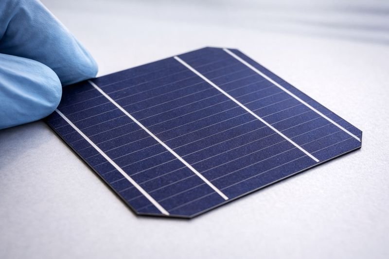
At the Fraunhofer Institute for Solar Energy Systems in Freiburg, Germany, a test cell no larger than a postage stamp sits inside a solar simulator. A lamp tuned to replicate the spectral output of the sun switches on. Within microseconds, electrons inside the silicon wafer begin moving in a single direction, and a current flows through the measurement leads. No heat engine is running. Nothing mechanical is happening. The cell converts roughly 26 percent of the incoming light directly into electrical power, which is close to the best result achievable with silicon under laboratory conditions.
What makes this possible is not a discovery about light. It is a discovery about a class of materials that sits, electrically speaking, exactly halfway between a metal and an insulator.
The short version: Semiconductors have a band gap, an energy threshold a photon must exceed to knock an electron free and make it available to carry current. Silicon’s band gap of 1.1 electron-volts aligns well with the peak of the solar spectrum, allowing it to absorb most visible and near-infrared light. In a solar cell, a deliberately engineered internal electric field then forces those freed electrons to travel in one direction rather than recombining at random, producing a sustained electrical current. Under real-world outdoor conditions, commercial silicon cells convert between 18 and 22 percent of incoming sunlight into electricity.
Table of Contents
Why Semiconductor Band Gaps Determine What Light Gets Absorbed
Electrical conductivity is not simply on or off. The distinction between a metal, a semiconductor, and an insulator comes from the quantum mechanical structure of the material, specifically from how electrons are arranged in energy bands and how much energy separates the occupied states from the states where electrons can move freely.
In a metal like copper, electrons at the top of the energy distribution already occupy the conduction band. They move with almost no encouragement, which is why copper wires carry current so efficiently. In an insulator like quartz glass, a wide gap separates the highest occupied states from the conduction band. Visible light photons do not carry enough energy to bridge it, which is why glass is transparent and does not conduct. Semiconductors sit between these two extremes. Their gap is narrow enough that photons of visible and near-infrared light can bridge it, but wide enough that the material is not a conductor in the dark.
The Energy Structure That Controls Absorption
Every crystalline solid has a valence band, the range of energies where electrons normally reside bound to atoms, and a conduction band, the range where electrons can move freely through the lattice. Between them is the forbidden gap, a range of energies no electron in the pure crystal can occupy. The width of this gap is the band gap, measured in electron-volts (eV).
For silicon, the band gap is 1.1 eV. Gallium arsenide, used in high-efficiency space cells, has a band gap of 1.42 eV. Cadmium telluride, the basis of a widely used thin-film technology, sits at 1.44 eV. Each value determines which photon energies can be absorbed and which pass through the material entirely.
Calculating the Absorption Threshold
A photon carries energy proportional to its frequency, described by Planck’s equation:
E = h x f
Where E is photon energy in joules, h is Planck’s constant (6.626 x 10^-34 joule-seconds), and f is frequency in hertz. Converting to electron-volts and expressing in terms of wavelength makes the result more useful for solar applications. A photon at 1100 nm, in the near-infrared, carries exactly 1.13 eV, which is just enough to push an electron across silicon’s 1.1 eV gap. A photon at 500 nm, in the green part of the visible spectrum, carries approximately 2.48 eV, well above the threshold.
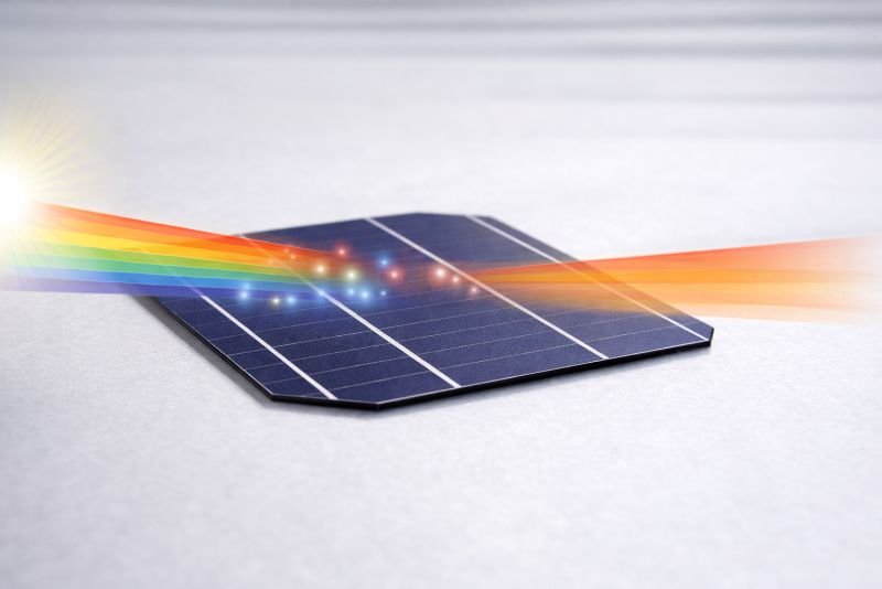
That excess energy matters. When a 2.48 eV photon knocks an electron across a 1.1 eV gap, the extra 1.38 eV is deposited as heat into the crystal lattice within picoseconds. It does not contribute to electrical output. This thermalization loss is one of the main reasons no single semiconductor can convert more than a theoretical maximum of around 33 percent of sunlight into electricity, a constraint known as the Shockley-Queisser limit.
The p-n Junction: Giving Freed Electrons Somewhere to Go
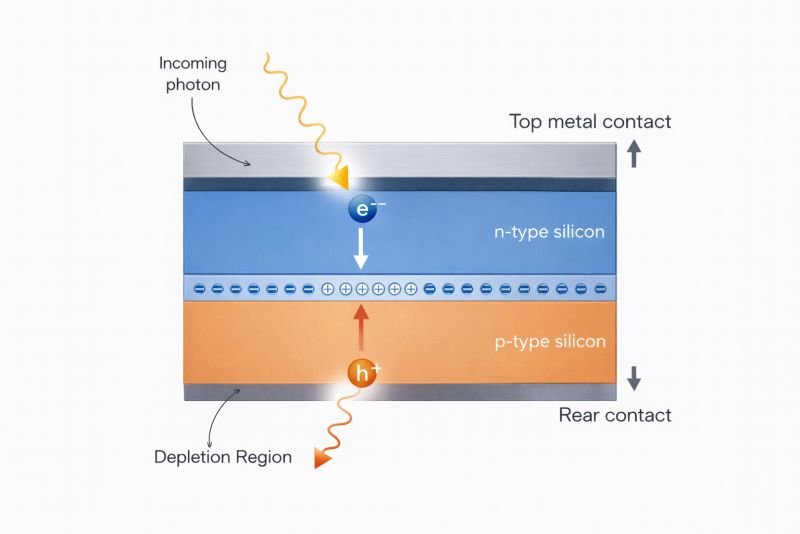
Freeing an electron from a valence bond is necessary but not sufficient. An electron knocked into the conduction band by a photon will recombine with the hole it left behind within nanoseconds unless something separates the two charges first. Solar cells work because a precisely engineered internal electric field performs exactly that separation, and the structure that creates it is called the p-n junction.
Pure silicon forms a stable crystal where all four valence electrons of each atom participate in bonding. Introducing small concentrations of impurity atoms changes this. Phosphorus has five valence electrons. When a phosphorus atom substitutes into the silicon lattice, four of its electrons bond normally, and one sits free with no bond to occupy. This is n-type silicon, named for the excess of free negative charge carriers. Boron has three valence electrons. A boron atom in the lattice creates a missing bond position, called a hole, which behaves as a mobile positive charge carrier. This is p-type silicon.
How the Depletion Region Forms
When n-type and p-type silicon layers are brought into direct contact, free electrons from the n-side diffuse across the boundary and fill holes on the p-side. This process leaves behind positively charged phosphorus ions on the n-side and negatively charged boron ions on the p-side. A region forms where the mobile carriers have been swept out, called the depletion region, and an electric field builds across it pointing from n to p.
This field is self-limiting. As more electrons diffuse across, the growing electric field increasingly opposes further diffusion. Equilibrium is reached when the electric field exactly balances the diffusion tendency. The resulting built-in potential across a typical silicon junction is around 0.7 volts.
From Separated Charges to Current
When a photon is absorbed in or near the depletion region and creates an electron-hole pair, the built-in electric field catches the carriers before they can recombine. Electrons are pushed toward the n-side. Holes are pushed toward the p-side. Connecting the two sides through an external circuit gives electrons a path to travel from the n-side contact to the p-side contact, completing the circuit through the external load. That directed flow of charge is the electrical current the cell produces.
How Semiconductor Material Choice Shapes Real Solar Cell Performance
The choice of semiconductor for a solar cell is primarily a choice about band gap, and that choice locks in a set of tradeoffs that cannot be engineered away. Too narrow a band gap and the cell captures more of the solar spectrum but wastes a large fraction of each high-energy photon’s energy as heat. Too wide a band gap and thermalization losses fall but a growing portion of the infrared spectrum passes through unabsorbed.
The Shockley-Queisser calculation shows that the theoretically optimal band gap for a single-junction cell exposed to the AM1.5 solar spectrum, the standard spectrum used for terrestrial testing, sits around 1.34 eV, giving a theoretical efficiency ceiling of about 33.7 percent. Silicon at 1.1 eV sits slightly below the optimum, with a theoretical ceiling closer to 30 percent. In practice, laboratory silicon cells have reached 26.7 percent, and the gap between that result and the theoretical limit reflects losses from surface recombination, contact resistance, and optical reflection.
| Semiconductor | Band Gap (eV) | Theoretical Max Efficiency | Current Commercial Use |
|---|---|---|---|
| Germanium | 0.67 | ~17% single junction | Bottom cell in multi-junction stacks |
| Silicon | 1.1 | ~30% | Dominant commercial technology |
| Gallium arsenide | 1.42 | ~33% | Space satellites, concentrator systems |
| Cadmium telluride | 1.44 | ~33% | Utility-scale thin-film panels |
| Perovskite (halide) | 1.5 to 1.7 | ~30 to 32% | Research and tandem architectures |
Silicon’s position at the top of the commercial market is not the result of having the best band gap. Gallium arsenide is closer to optimal and achieves higher efficiencies. Silicon dominates because it is the second most abundant element in Earth’s crust, because the semiconductor industry developed extraordinary expertise in processing it over seventy years of electronics manufacturing, and because its physical properties are more thoroughly understood than those of any other semiconductor. A fractionally better band gap in an expensive material cannot compete with that infrastructure.
Everything here is free. Readers are the reason it stays that way.
I make all of it alone, with no ads. If it is worth a coffee a month to you, that keeps the next one coming.
Keep it alive →Carrier Recombination and Why Semiconductor Purity Sets the Efficiency Ceiling
The built-in electric field of the p-n junction separates charge carriers only if they survive long enough to reach it. An electron generated deep in the p-type absorber must diffuse through the silicon lattice before the junction can catch it. If it encounters a defect, an impurity, or a crystal grain boundary along the way, it falls into a localized energy state inside the band gap and recombines with a hole without contributing to current. The average distance a minority carrier can travel before recombining is called the minority carrier diffusion length, and it is one of the key material quality metrics in photovoltaics.
In high-purity monocrystalline silicon, the minority carrier diffusion length can reach several hundred micrometers. In polycrystalline material with a high density of grain boundaries, it can fall below ten micrometers. A solar cell designed for a thin absorber layer in polycrystalline material produces far less current per photon absorbed.
The Purity Requirements That Follow From This Physics
Crystal defects and foreign atoms create trap states inside the band gap. Any impurity that introduces an energy level near the middle of the gap is particularly damaging because mid-gap states are the most effective recombination centers. Iron, copper, and nickel are especially harmful in silicon at concentrations above roughly one part per trillion by weight.
This is why solar-grade silicon requires purity levels that would have seemed extraordinary for any other industrial material a century ago. Standard metallurgical silicon used in steel alloys is around 98 percent pure. Solar-grade silicon is produced by converting silicon to trichlorosilane gas, purifying through repeated fractional distillation, and then depositing ultra-pure silicon by chemical vapor deposition. The result is material with total metallic impurity concentrations below one part per billion. The energy cost of this process is significant, and it historically dominated the embodied energy in a finished panel.
Surface Passivation and the PERC Architecture
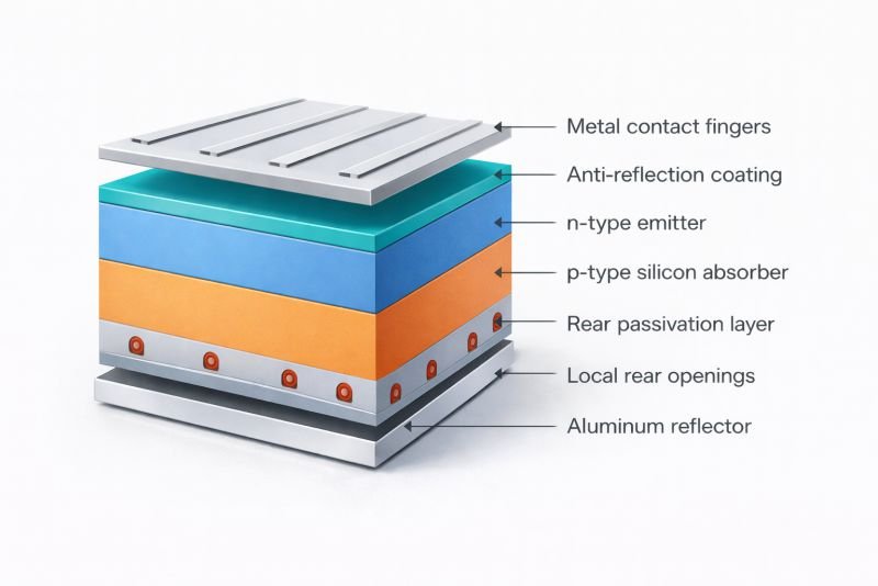
At the surface of a silicon wafer, the crystal lattice ends abruptly. Dangling silicon bonds at the surface create a dense band of trap states that would cause catastrophic recombination without treatment. Modern cells apply passivation layers, thin films of silicon dioxide, silicon nitride, or aluminum oxide, that chemically satisfy the dangling bonds and suppress surface recombination.
The passivated emitter and rear cell structure, universally referred to as PERC, extends passivation to both the front and rear surfaces of the wafer. PERC cells also incorporate a rear reflector that bounces unabsorbed photons back through the absorber for a second pass, recovering some of the light that would otherwise escape. PERC is now the dominant silicon cell architecture in commercial production, accounting for the majority of panels manufactured globally.
Reading the I-V Curve: How Semiconductor Properties Appear in Cell Measurements
Connecting a solar cell to a variable load and plotting the current that flows against the voltage across the cell produces the current-voltage curve, abbreviated as the I-V curve. This graph encodes the performance of every semiconductor property discussed so far in a form engineers can measure directly.
At zero external resistance, the maximum current flows through the short circuit. This short-circuit current, written Isc, is directly proportional to how many photons the cell absorbs and what fraction of generated carriers the junction successfully collects. At the opposite extreme, with no current flowing at all, the full open-circuit voltage Voc appears across the junction. The product of Isc and Voc sets an upper bound on what the cell could deliver in theory.
Real cells fall short of that upper bound. Series resistance in the metal contacts and semiconductor layers causes voltage to drop as current increases. Shunt resistance from microscopic leakage paths through defects allows some current to bypass the external load entirely. The fill factor, abbreviated FF, quantifies how closely the actual I-V curve approaches the rectangular shape of an ideal cell. Commercial silicon cells achieve fill factors between about 0.78 and 0.85.
The power conversion efficiency combines all three quantities:
PCE = (Voc x Isc x FF) / Pin
Where PCE is the fraction of incident light power converted to electrical power, and Pin is the total light power per unit area striking the cell. For a good commercial silicon cell under standard test conditions at 1000 W/m², Voc might be 0.64 V, Isc might be 39 mA/cm², and FF might be 0.81. Substituting:
PCE = (0.64 x 0.039 x 0.81) / 0.1 = 0.0202 / 0.1 = 20.2 percent
That calculation accurately describes a well-manufactured silicon panel operating under real-world conditions. Every semiconductor property in the cell, from band gap to minority carrier lifetime to surface passivation quality, contributes to one or more of the three terms in this equation.
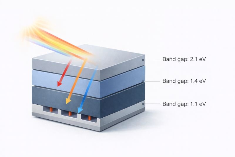
Multi-Junction Cells: Stacking Semiconductors to Escape the Single-Junction Limit
The Shockley-Queisser limit applies to a single semiconductor absorbing a single range of the solar spectrum. A different architecture breaks the constraint: stack multiple semiconductors on top of each other, each with a different band gap, each absorbing a different slice of the spectrum. The result is a multi-junction cell that extracts useful energy from a far wider portion of the incoming light.
In practice, the top cell uses a wide-band-gap semiconductor to absorb high-energy blue and ultraviolet photons. Photons that pass through travel into the middle cell, which absorbs green and red photons. Remaining near-infrared photons reach the bottom cell, which has the narrowest band gap and absorbs what the layers above transmitted. Each cell produces its own voltage, and connecting them in series adds the voltages together.
The highest laboratory efficiency recorded for any solar cell is 47.6 percent, achieved by the Fraunhofer Institute in 2022 using a four-junction III-V semiconductor cell under concentrated sunlight equivalent to approximately 665 times normal intensity. The semiconductors in such cells, compounds built from elements in groups 13 and 15 of the periodic table including gallium, indium, arsenic, and phosphorus, can be grown with precise band gap control by adjusting composition. Manufacturing cost is orders of magnitude higher than silicon, which limits these cells to space satellites and concentrating photovoltaic systems.
The commercially relevant version of the multi-junction idea is the tandem cell, where a perovskite absorber layer is deposited on top of a standard silicon bottom cell. Perovskite compounds are tunable: changing the halide composition adjusts the band gap continuously between roughly 1.2 and 2.3 eV, allowing the top cell to be engineered to complement silicon precisely. Laboratory tandem cells have already exceeded 33 percent efficiency, breaking through the single-junction silicon limit. Several manufacturers are in early commercial production, and if manufacturing yield improves, tandem architecture may redefine what efficiency is achievable on a standard rooftop panel.
Semiconductors in Solar Cells and the Technologies Being Built Around Them
The physics established in silicon photovoltaics, band gap absorption, junction-driven carrier separation, surface passivation, and multi-junction stacking, defines the design space for every photovoltaic technology under active development.
Perovskite single-junction cells have reached laboratory efficiencies of 26.1 percent, competitive with the best silicon cells ever made, despite using a material that was not considered for photovoltaics until 2009. Their unusual defect tolerance, where crystal imperfections that would be catastrophic in silicon cause only modest losses, is not yet fully understood at the atomic level and remains an active research question. Quantum dot absorbers offer a different route: semiconductor nanocrystals whose band gap is controlled by particle size through quantum confinement rather than material composition, opening the possibility of tuning the absorption edge across a continuous range without changing the chemistry. Organic photovoltaics use carbon-based semiconductor molecules as absorbers, enabling cells deposited from solution onto flexible plastic substrates at far lower temperatures than crystalline silicon processing requires.
Each of these directions is an extension of the same underlying physics. The semiconductor is not peripheral to solar energy conversion. It is the physical mechanism by which light becomes current, and every meaningful efficiency improvement in photovoltaics comes from understanding that mechanism more deeply and exploiting it more precisely.
You read the whole thing.
That is rarer than it should be, and it is the exact kind of attention I built this archive for. I make every piece alone, with no ads and no investor deciding what gets written. If you want the next machine taken apart like this one, you can help me make it.
A coffee a month is enough to keep it free for everyone.
Prefer crypto or a one time gift? Other ways to give →
Technologies Related to This Concept
| Technology | Concept |
|---|---|
| Solar Power-Generating Textiles for Smart Clothing | Concept: Fabrics woven with photovoltaic fibers that generate electricity from sunlight, powering wearable electronics. |
| Building-Integrated Photovoltaics: The Future of Urban Architecture | Concept: Incorporating solar panels into building materials like windows and facades. |
| Transparent Solar Windows | Concept: Windows made from transparent photovoltaic glass that generate electricity. |
| Dynamic Glass Buildings with Solar Control | Concept: Glass that adjusts transparency to generate energy and regulate building temperature. |
| Photovoltaic Building Facades with Energy Paints | Concept: Skyscrapers coated with solar paints to transform entire facades into energy generators. |