
There is a roof in Freiburg that has been generating electricity since 1999. The Fraunhofer Institute for Solar Energy Systems installed it as a long-term performance test, and after more than two decades the panels are still producing power within a few percent of their original output. What the test confirmed is not that solar cells are perfect. It confirmed that silicon is astonishingly stable and that the losses baked into the basic design are also astonishingly durable. The same inefficiencies that existed in 1999 are still present today in most commercially installed panels.
That is the real problem nanotechnology is trying to solve. Not durability. Not cost, at least not directly. The target is the physics of light conversion itself, which in a standard silicon cell wastes roughly three-quarters of the energy arriving from the sun before a single electron reaches the external circuit.
The short version: Conventional silicon solar cells convert around 22% of incoming sunlight into electricity. The theoretical ceiling for a single-junction silicon cell is 33%, set by the Shockley-Queisser limit. Nanomaterials can push past that ceiling by manipulating quantum mechanical behavior at scales below 10 nanometers, allowing cells to absorb more of the solar spectrum and extract more energy from each absorbed photon. Lab cells using quantum dot architectures have already exceeded 40% efficiency under concentrated light.
Table of Contents
Why Silicon Solar Cells Waste Most of the Sun
A silicon solar cell absorbs a photon, and if that photon carries enough energy, it knocks an electron loose from its position in the crystal lattice. The electron moves through the material and eventually exits as electrical current. The process is elegant and the physics behind it has been understood since Einstein’s 1905 paper on the photoelectric effect.
The problem is that the sun does not send a single wavelength of light. It sends a broad spectrum, from infrared through visible to ultraviolet, each wavelength carrying a different quantity of energy per photon. Silicon responds only to photons above a specific energy threshold, called the bandgap, which sits at 1.1 electron volts. Photons below that threshold pass through the material entirely without doing anything useful. Photons above the threshold are absorbed, but the excess energy above the bandgap is not converted to electricity. It becomes heat.
The Shockley-Queisser Limit and Why It Matters
In 1961, William Shockley and Hans-Joachim Queisser calculated the maximum efficiency any single-junction solar cell could achieve. Their result was approximately 33% for a cell operating under standard solar illumination. The losses below that ceiling are not engineering failures. They are consequences of using a single semiconductor with a fixed bandgap to handle a spectrum of photons with widely varying energies.
The calculation follows from thermodynamics and the shape of the solar spectrum. A cell optimized for the peak of the spectrum underperforms at the edges. A cell that captures the edges sacrifices efficiency at the peak. There is no single bandgap that handles all wavelengths well.
Nanotechnology addresses this directly, not by improving silicon, but by replacing or supplementing the fixed bandgap with materials whose electronic properties can be tuned by adjusting their physical dimensions.
Quantum Confinement: The Physics That Makes Nanomaterials Different
When a semiconductor is shrunk to dimensions smaller than roughly 10 nanometers, something changes in the physics. Electrons inside the material can no longer move as freely as they do in a bulk crystal. They become spatially confined, and that confinement forces them into discrete energy states rather than the continuous bands that govern electron behavior in larger pieces of material.
This is quantum confinement, and its practical consequence is remarkable: the bandgap of the material becomes a function of its size. A quantum dot made from cadmium selenide that is 2 nanometers in diameter has a different bandgap than one that is 5 nanometers in diameter, even though both are made of exactly the same atoms in exactly the same arrangement. Change the size, change the bandgap.
Tuning the Bandgap by Changing the Dot
The relationship between size and bandgap follows from the particle-in-a-box model in quantum mechanics. The energy of the ground state scales inversely with the square of the confinement dimension. Written out:
E = E_bulk + (h² / 8m* d²)
Where E is the effective bandgap, E_bulk is the bandgap of the bulk material, h is Planck’s constant (6.626 × 10⁻³⁴ J·s), m* is the effective mass of the electron in the material, and d is the diameter of the quantum dot.
Working through this with cadmium selenide: the bulk bandgap is 1.74 eV. A quantum dot 3 nanometers in diameter shifts the effective bandgap up toward 2.1 eV, absorbing blue light efficiently. A dot 6 nanometers in diameter sits closer to 1.9 eV, capturing more of the green range. A dot at 8 nanometers approaches the bulk value and handles orange and red wavelengths. The same material, three different sizes, three different absorption windows covering a significant portion of the solar spectrum.
That tunability is the core advantage. A solar cell incorporating quantum dots of different sizes can, in principle, be engineered to absorb light across a much wider band than any single-junction bulk semiconductor.
How Nanomaterials Are Applied in Photovoltaic Cells
There are several distinct approaches to integrating nanotechnology into solar cells, each targeting a different inefficiency in the conversion chain.
Quantum Dot Solar Cells
The most direct application places quantum dots as the light-absorbing layer itself. Colloidal quantum dots, grown as nanocrystals suspended in solution, can be deposited onto a substrate in thin films using relatively low-cost processes. Unlike silicon wafer production, which requires high-temperature processing and ultra-clean manufacturing environments, quantum dot films can be applied at room temperature using methods similar to inkjet printing.
The challenge is getting the electrons out efficiently once they have been generated. Quantum dots in close proximity can exchange energy non-radiatively, which wastes the absorbed photon energy as heat before the electron can be extracted. Engineering the spacing and surface chemistry of the dots to minimize these losses while maintaining electrical conductivity between particles is a problem that research groups have been working on since the early 2000s.

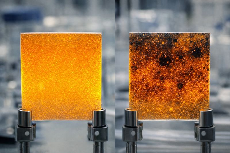
Perovskite Solar Cells with Nanoscale Architecture
Perovskite materials, named for their crystal structure rather than their composition, have absorbed an enormous amount of research attention over the past decade. Their efficiency in lab conditions rose from around 3% in 2009 to over 25% by the early 2020s, a rate of improvement with no precedent in the history of photovoltaics.
The performance gains come partly from the material’s intrinsic properties and partly from nanoscale engineering of the interfaces between layers. A perovskite cell consists of multiple layers, and the boundaries between them are sites of recombination losses, where electrons and holes find each other and annihilate before reaching the external circuit. Inserting nanoscale passivation layers at these interfaces, thin films just one or two nanometers thick, reduces the defect density and raises the voltage the cell can deliver.
Multi-Junction Cells Using Nanowire Architectures
A different approach stacks multiple absorbing layers, each tuned to a different part of the spectrum. Conventional multi-junction cells do this with bulk semiconductor alloys, and the best of them exceed 47% efficiency under concentrated sunlight. Nanowire architectures attempt to achieve similar multi-junction behavior with less material by growing vertical semiconductor wires with diameters below 100 nanometers.
The wires can be grown with varying composition along their length, creating multiple bandgap regions within a single structural element. Light enters the tip, and different wavelengths are absorbed at different points along the wire, each at the bandgap most suited to it. Less recombination, less wasted thermal energy, and a geometry that concentrates light into the absorbing volume.
| Approach | Primary Advantage | Key Challenge | Lab Efficiency |
|---|---|---|---|
| Quantum dot films | Tunable bandgap, low-temperature deposition | Carrier extraction losses between dots | ~18% single junction |
| Perovskite with nanolayers | Rapid efficiency gains, scalable | Long-term stability, lead content | ~26% lab cells |
| Nanowire multi-junction | Broad spectrum coverage, low material use | Manufacturing complexity at scale | ~35% concentrated light |
| Organic nanostructures | Flexible substrates, low cost | Lower efficiency, UV degradation | ~12% |
Everything here is free. Readers are the reason it stays that way.
I make all of it alone, with no ads. If it is worth a coffee a month to you, that keeps the next one coming.
Keep it alive →Multiple Exciton Generation: More Than One Electron Per Photon
There is a phenomenon in quantum dot materials that has no equivalent in bulk semiconductors, and it is one of the more consequential things nanotechnology brings to photovoltaics.
In a bulk silicon cell, a high-energy photon, one carrying two or three times the bandgap energy, generates a single electron-hole pair. The excess energy above the bandgap goes directly into heating the lattice, a process called thermalization. That heat is not recoverable.
In certain quantum dot materials, a high-energy photon can instead generate two electron-hole pairs. The process is called multiple exciton generation. The excess energy, rather than heating the crystal, drives a second ionization event within the quantum dot itself. Two charges extracted per absorbed photon effectively doubles the current from high-energy photons, without needing to absorb any additional light.
The efficiency consequence is significant. Theoretical calculations suggest that a solar cell exploiting multiple exciton generation could reach efficiencies approaching 44% under standard illumination, well above the Shockley-Queisser limit. The practical results are more modest. Research cells incorporating the effect have demonstrated measurable improvements in photocurrent at short wavelengths, but translating those improvements into whole-cell efficiency gains has proven difficult. The competing loss mechanisms, particularly charge extraction losses at dot surfaces, tend to absorb much of the benefit before it reaches the circuit.
This is one of those situations where the physics is clearly doing something useful and the engineering has not yet caught up. The effect is real. The gain is real in isolated measurements. Getting it out of the dot and into the wire is the part that remains genuinely hard.
What Limits Nanotechnology in Solar Cells Today
The physics is not the binding constraint. This is worth stating plainly, because it is easy to read about 44% theoretical efficiency ceilings and assume the technology is on the verge of transforming the industry. It is not. The engineering problems are real, and some of them are stubborn.
Surface Defects and Recombination Losses
A quantum dot has an extraordinarily high ratio of surface area to volume. In a 3-nanometer dot, roughly 15% of all atoms sit on the surface. Surface atoms have unsatisfied chemical bonds, called dangling bonds, that act as traps for electrons. A generated electron falls into a trap and recombines without producing useful current. More traps means lower efficiency.
Surface passivation, coating the dot’s outer layer with ligands or shell materials that satisfy those dangling bonds, is one of the most active research areas in the field. Core-shell quantum dot architectures, where a thin shell of a wider-bandgap material surrounds the active core, have demonstrated significant reductions in trap-state density. The improvement translates directly into longer carrier lifetimes and higher photocurrent extraction.
Stability Under Continuous Illumination
Solar cells operate under sustained UV exposure for decades. Bulk silicon handles this with known degradation rates that are slow enough to be commercially acceptable. Perovskite materials degrade faster, particularly when exposed to moisture, and the best performing perovskite compositions contain lead, which complicates regulatory approval for large-scale deployment. Quantum dot films have their own stability challenges; the organic ligands used to passivate surfaces can detach over time, increasing trap density and reducing efficiency.
The stability problem is not unsolvable. Research groups have demonstrated perovskite cells retaining over 90% of initial efficiency after 1000 hours of illumination, which represents meaningful progress but remains short of the 25-year performance warranties that standard silicon panels carry. Nanomaterials need to reach comparable stability benchmarks before utility-scale deployment becomes realistic.
From Lab Cell to Manufactured Panel
A lab cell achieving 26% efficiency with a perovskite architecture is not the same as a manufactured panel achieving 26% efficiency. The gap between the two is where most of the real work in photovoltaics happens, and it is larger than it looks from the outside.
Lab cells are small, often less than 1 square centimeter, fabricated under carefully controlled conditions with no tolerance for the imperfections that appear when processes are scaled up. Larger cells introduce more defects at grain boundaries. Interconnecting cells into a module introduces resistive losses. Encapsulation layers add cost and can affect optical transmission. The efficiency number in a journal paper is the ceiling of what the physics can deliver. The efficiency number on a commercial panel is what survives the full manufacturing and assembly process.
For quantum dot and perovskite nanotechnology in solar cells, the path to manufactured panels requires solving deposition uniformity at meter scales, developing encapsulation methods that exclude moisture without reducing optical throughput, and establishing long-term field performance data sufficient to support commercial warranties. None of these is a fundamental physics problem. All of them are expensive engineering problems that take years of development capital to solve.
Silicon took roughly 40 years to get from the Bell Labs demonstration to commercial viability. Perovskites are roughly 15 years into that journey. The trajectory is faster partly because the research infrastructure is larger and partly because the manufacturing tooling for thin-film deposition already exists from earlier photovoltaic generations.
Where Nanotechnology in Solar Cells Is Taking Photovoltaics
The Shockley-Queisser limit has been the fixed ceiling of solar cell design for sixty years. Nanotechnology is the first approach that addresses it at the level of fundamental physics rather than incremental materials optimization.

The near-term trajectory points toward tandem architectures, where a perovskite or quantum dot layer handles the high-energy end of the spectrum while silicon continues doing what it does reliably at the low-energy end. Several research groups have demonstrated perovskite-silicon tandem cells exceeding 33% efficiency in lab conditions, which already clears the single-junction ceiling. Getting those architectures through a manufacturing process and onto a roof for three decades is the engineering work that remains.
Further out, multiple exciton generation opens a conceptually different path. If surface passivation methods improve to the point where the effect can be harvested efficiently at the cell level, the same quantity of sunlight could drive substantially more current without increasing panel area. That matters most in space-constrained installations, dense urban environments, and any application where the cost per watt is less important than the power per square meter.
The deeper significance of quantum confinement as a principle is that it gives engineers a variable that did not exist before. Bulk semiconductor design is largely fixed by the periodic table. Nanomaterials introduce size as a design parameter, which means absorption spectra can be engineered rather than inherited. That is a qualitative change in what photovoltaic design is capable of, and its consequences for solar technology are still being worked out.
You read the whole thing.
That is rarer than it should be, and it is the exact kind of attention I built this archive for. I make every piece alone, with no ads and no investor deciding what gets written. If you want the next machine taken apart like this one, you can help me make it.
A coffee a month is enough to keep it free for everyone.
Prefer crypto or a one time gift? Other ways to give →
Technologies Related to This Concept
| Technology | Concept |
|---|---|
| Energy-Producing Paints for Buildings | Concept: Paint infused with photovoltaic nanoparticles that convert walls and roofs into solar panels. |
| Energy-Harvesting Road Markings with Solar Paint | Concept: Roads painted with solar-absorbing materials that generate electricity from sunlight. |
| Solar Power-Generating Textiles for Smart Clothing | Concept: Fabrics woven with photovoltaic fibers that generate electricity from sunlight, powering wearable electronics. |
| Solar-Powered Tents for Off-Grid Living | Concept: Camping tents made from solar fabrics that provide electricity for lighting and device charging. |
| Energy-Generating Tarp Covers for Disaster Relief | Concept: Solar fabric tarps that provide shelter and electricity in emergency situations. |